On Friday, May 12, 2017, the world woke up to realize it was under attack from an enemy that was undermining parts of its most critical infrastructure. A cryptoworm had burrowed itself into more than 200,000 computers worldwide – encrypting data and demanding ransom payments.
The National Health Service (NHS) hospitals in England and Scotland were among the victims. From one moment to the next, up to 70,000 devices stopped working, including MRI scanners, blood storage refrigerators, and surgical equipment.
The cyberattack was named WannaCry and remains the most notable example of the potential consequences of memory vulnerabilities. The problem is that program languages such as C and C++ are not memory-safe. Identifying the weaknesses in millions of lines of (legacy) code is next to impossible, which means there will always be a backdoor open for anyone determined to get in.
According to the Microsoft Security Research Center, a security-optimized CPU architecture could weed out at least 70% of the memory vulnerabilities that they came across over the years. This is what the Morello research program is seeking to address by implementing hardware capability technology using concepts from the University of Cambridge’s CHERI project. The research program aims to develop and evaluate a prototype architecture, led by Arm with funding from the UK government’s digital-security-by-design (DSbD) initiative.
Powerful weapon against cybercrime
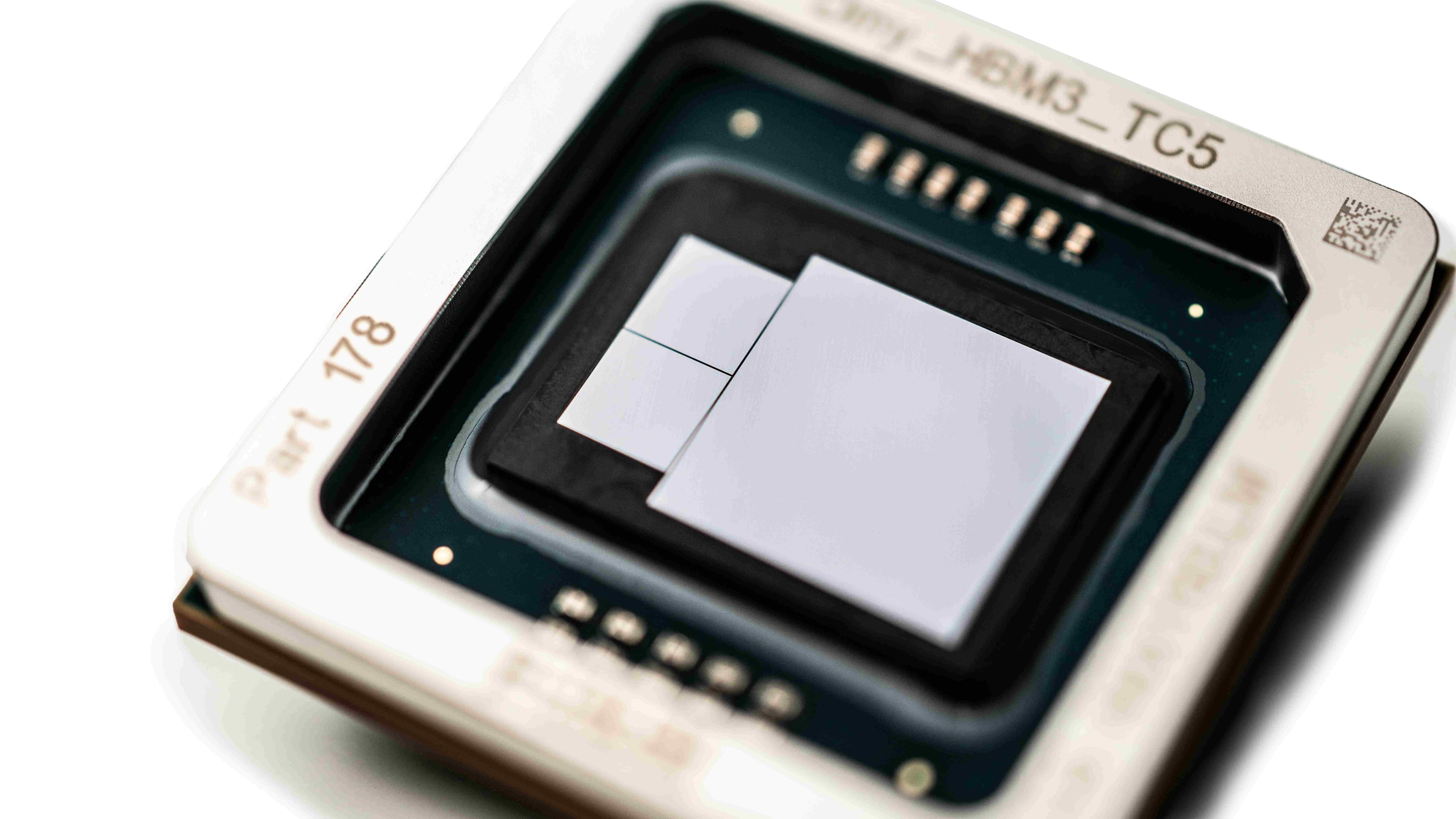
Morello is based on the concept of Capability Hardware Enhanced RISC Instructions (CHERI), developed at the University of Cambridge. It has the potential to prevent most attacks exploiting memory vulnerabilities and therefore prevent attacks on digital infrastructure. But it will also require significant changes – not only in terms of hardware design but also for software programming. To assess these changes, Arm has designed a prototype system-on-chip (SoC) on a development board, a major step forward in progressing this research. Interested parties, both from industry and academia, including software developers, can use it to evaluate the new architecture and find out what its implications are. Global industry leaders such as Microsoft and Google are collaborating on the program.
The SoC contains four powerful CPUs so that the impact of demanding software workloads can be properly investigated. In addition, Morello is a versatile platform that can be used for a range of workloads from smartphones to data centers, and that aims to support a broad range of operating systems from Linux to Android and CheriBSD (Developed by University of Cambridge).
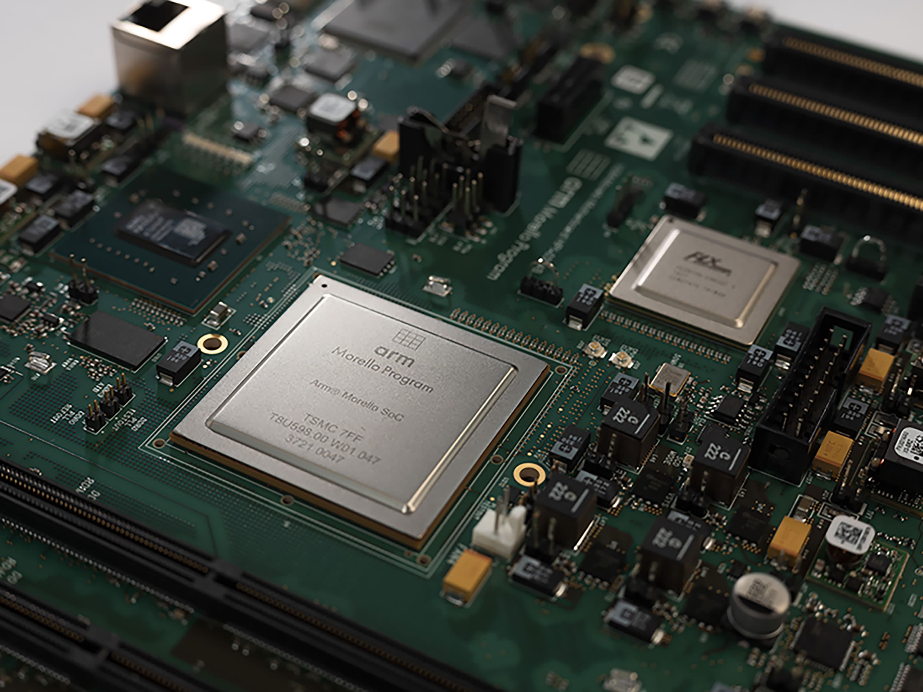
Morello SoC on a board
Partner with expertise and connections
Morello is more than a concept; it’s a real prototype implementation in silicon. For that, Arm decided to collaborate with a specialist partner to fabricate the complex Morello SoC. Arm reached out to IC-Link, imec’s ASIC development division. IC-Link supported Arm through its expertise and its access to the silicon ecosystem.
Mark Inskip, Morello Program Manager, Arm: “ The complexity of the Morello chip extends to the SoC packaging, which requires development of an eighteen-layer substrate. IC-Link managed the design process, working closely with the Arm team. Once the design was ready, IC-Link enabled the manufacturing of the substrate with Kyocera.”
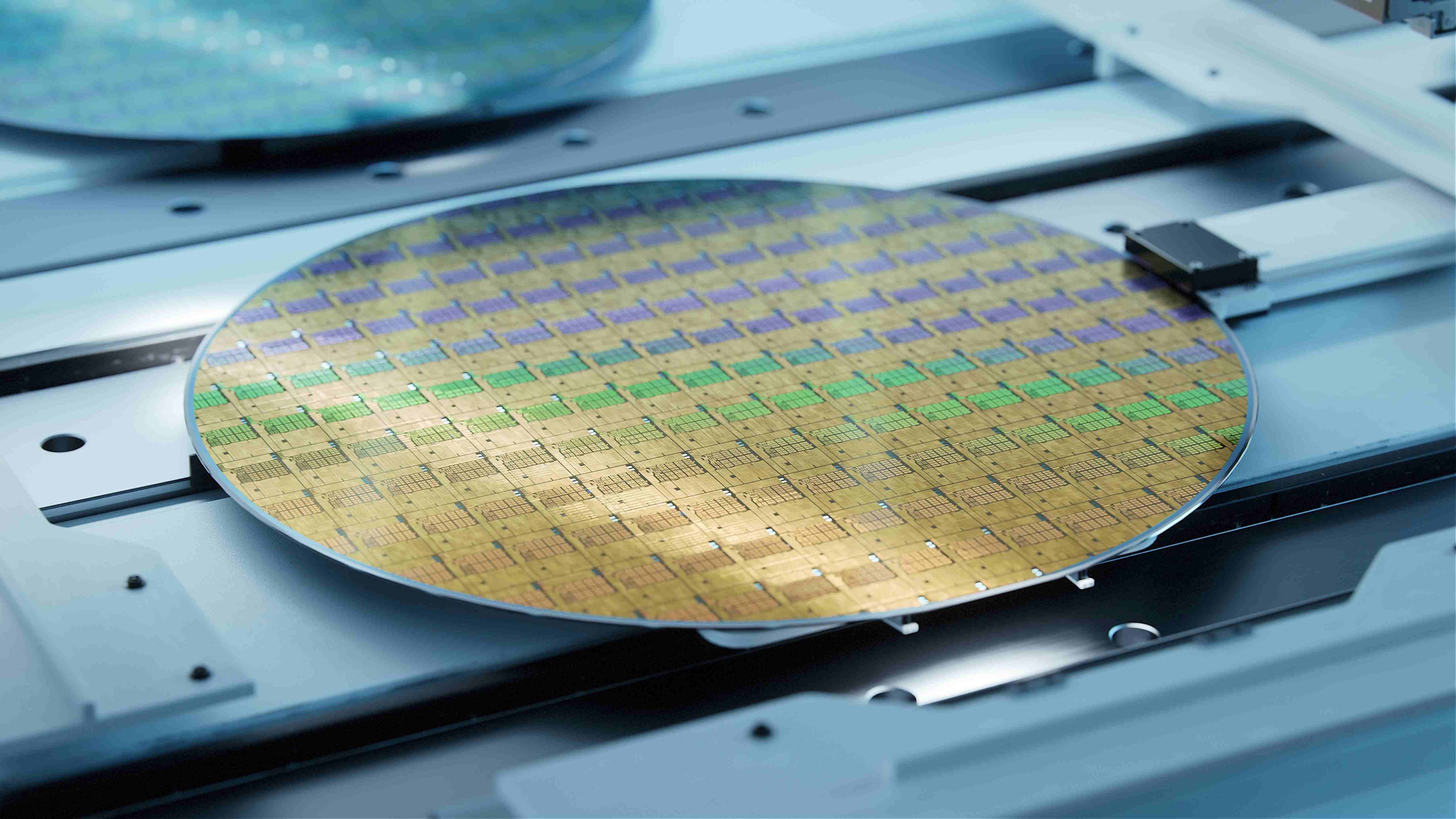
IC-Link also facilitated easy access to a TSMC full mask set tape-out. The team supported with some logistical and administrative challenges around the focused ion beam (FIB) process that was needed to validate a design fix at one of the top metal layers, saving time and effort on the Arm side.
This was all possible thanks to the extended partner network of IC-Link who can provide all the essential services in the supply chain in the semiconductor manufacturing.
This critical support and knowledge provided by IC-Link, allowed the Arm team to focus on their own areas of expertise, and was an essential ingredient in the project’s success and the delivery of the prototype Morello development board.
Want to know more about the Morello project? Visit the website

Mark has over 30 years' experience in the semiconductor industry. He has worked at Arm for over a decade, most recently as a Program Director. He started his career at Philips Semiconductors as an IC Designer before progressing to engineering and project management roles. A Chartered Engineer and Senior Member of the IEEE, he holds an honours degree in Electronic Engineering.
Published on:
16 February 2022


