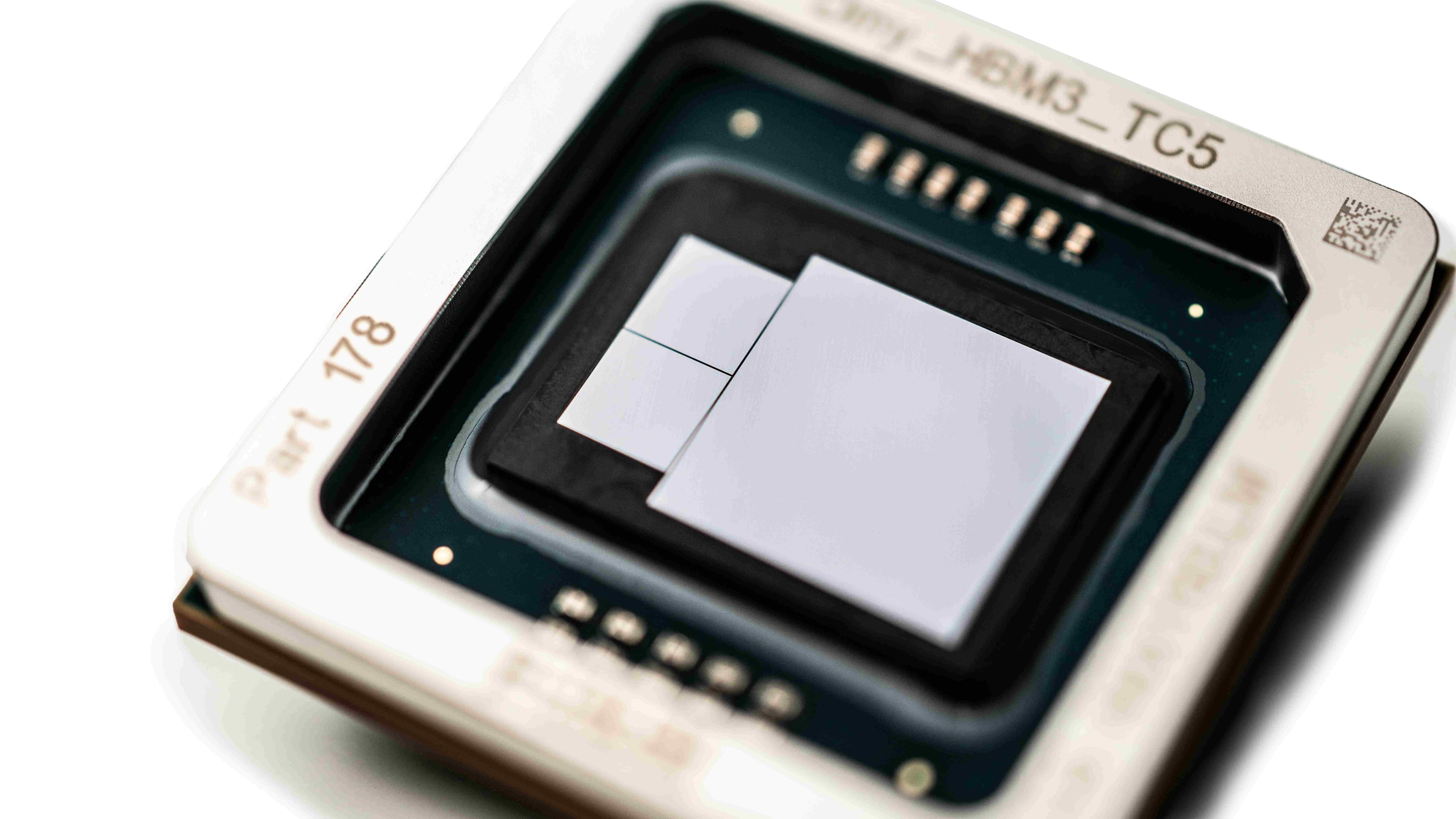
The production of chips using the N3 process, sometimes referred to as 3 nanometer (nm), is ramping up. Its features are now accessible to more companies than just the tech giants. And for more purposes than flashier smartphones and more powerful servers.
IC-Link has already completed several N3 process tape-outs with TSMC for our customers. With the new tech available, there are many cases in which companies can gain a competitive advantage by using N3.
But what is N3 and when does it make sense to use it? Read this article for a general introduction. And don’t hesitate to get in touch to find out if it’s right for your next ASIC.
The next step in chip scaling
Continued transistor scaling is the semiconductor industry’s most important tool to keep up with Moore’s law. The N3 is the next logical step in this process.
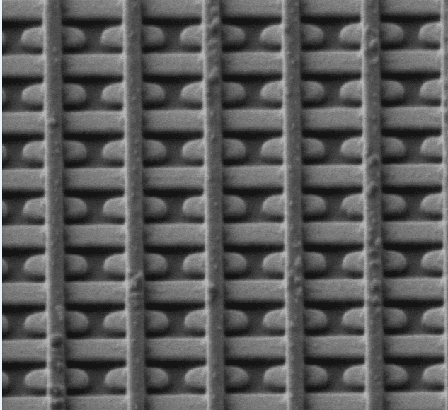
Compared to the previous N5 node, TSMC’s N3 technology is a new process rather than a mere improvement. It uses innovations such as the finest generation of FinFET technology and EUV lithography to achieve:
- 10-15% performance improvement at the same power and transistor count
- 20-30% reduced power consumption at the same frequency and complexity
- 1.6 times higher logic density
Impressive numbers. But do they warrant switching to this node for your upcoming ASIC project? Because, of course, that switch requires significant resources – especially at the beginning.
Our answer? It depends.
To N3 or not to N3
One of the services IC-Link provides its customers is a tailored technology selection. The purpose should never be to flaunt an ‘advanced’ technology node, but to choose one that fits your technology and market requirements – at the best price/performance ratio. And this principle remains true for the most advanced technology node that’s currently available.
The cases that make the most sense for N3 are those that require the highest computing power. But the N3 process is just as much about miniaturization and energy efficiency. In that respect, it can be the prime enabler of emerging new use cases around high-performance computing, network applications and, in the future, edge AI and smart sensors – especially if you’re an ambitious start-up, working in fintech or data- and telecom.
And if that’s the case, it’s important to move fast.
Short- and long-term gains of the N3 process
As we said earlier, starting a project in TSMC’s N3 technology node necessitates significant investments in all steps of the ASIC development process – from design to manufacturing.
However, here are two things to keep in mind when you’re financially balancing your options.
- The first-mover advantage in emerging tech markets such as those described above, outweighs the extra costs that come with investing in N3 design and manufacturing.
- Over time, when scaling up to high-volume production, the cost-efficiency automatically increases, because the price per piece falls as you fit more chips on a wafer.
In short, if N3 is the right technology for you, the sooner you get started the better. And by partnering with IC-Link, you minimize the risks that traditionally come with being an early adopter.
A clear path to N3 technology
IC-Link is the ASIC development division of imec, the world’s leading semiconductor R&D hub. It’s therefore in our DNA to be at the forefront of innovation. And our strong partnerships with leading foundries such as TSMC enable us to fulfill that ambition.
When it comes to N3 technology, we offer you a host of flexible turnkey services that cover all steps of the development process:
- ASIC design and IP services
- assembly and advanced package design services
- test, qualification, and production optimization services
- volume production with a tailored supply chain
Additionally, our comprehensive ASIC knowledge ensures that your technology specs are geared to your solution and its market opportunities.
Ready to grab the opportunities offered by the N3 process or more advanced nodes and propel your solutions to the forefront of the market?
Published on:
10 July 2024


