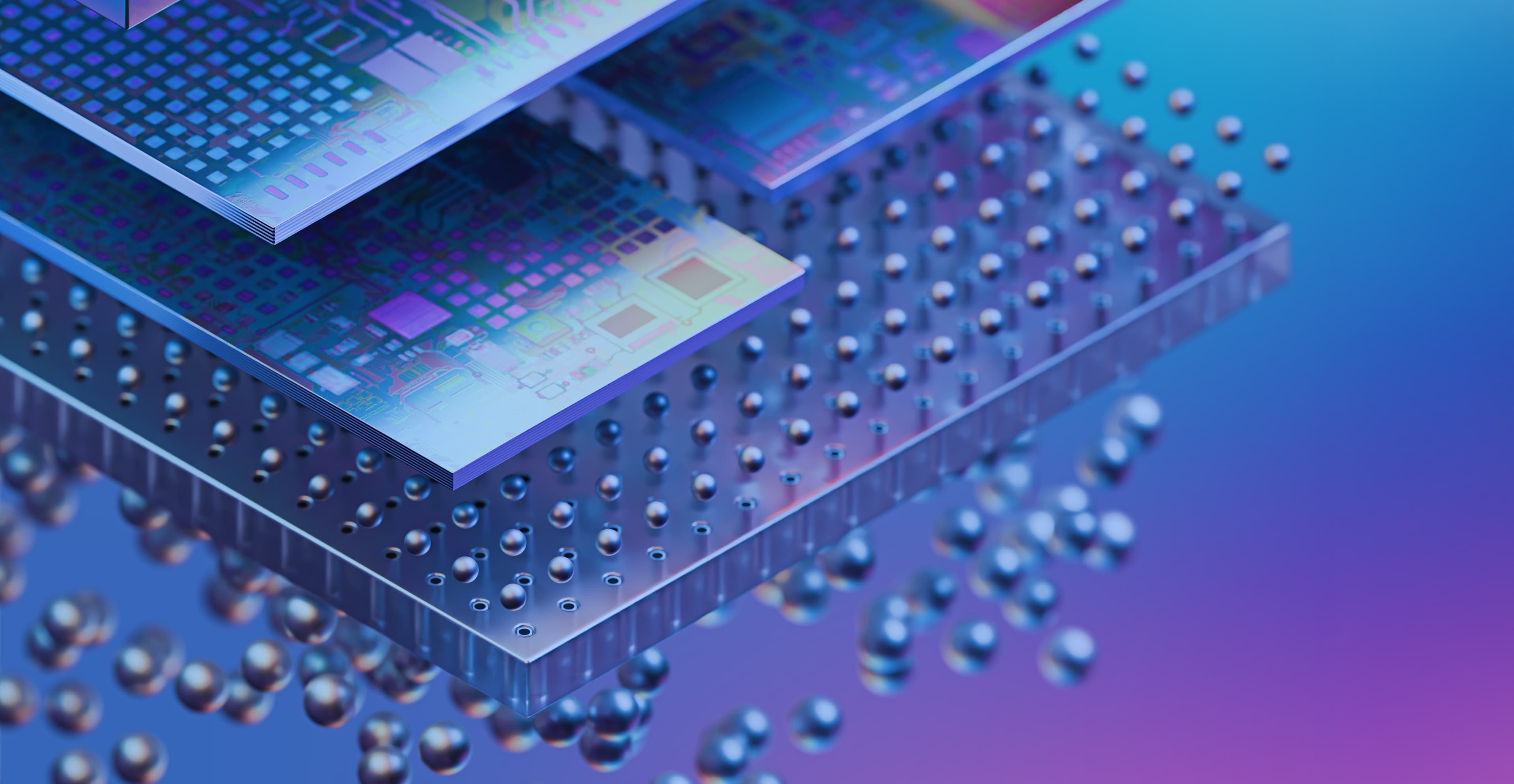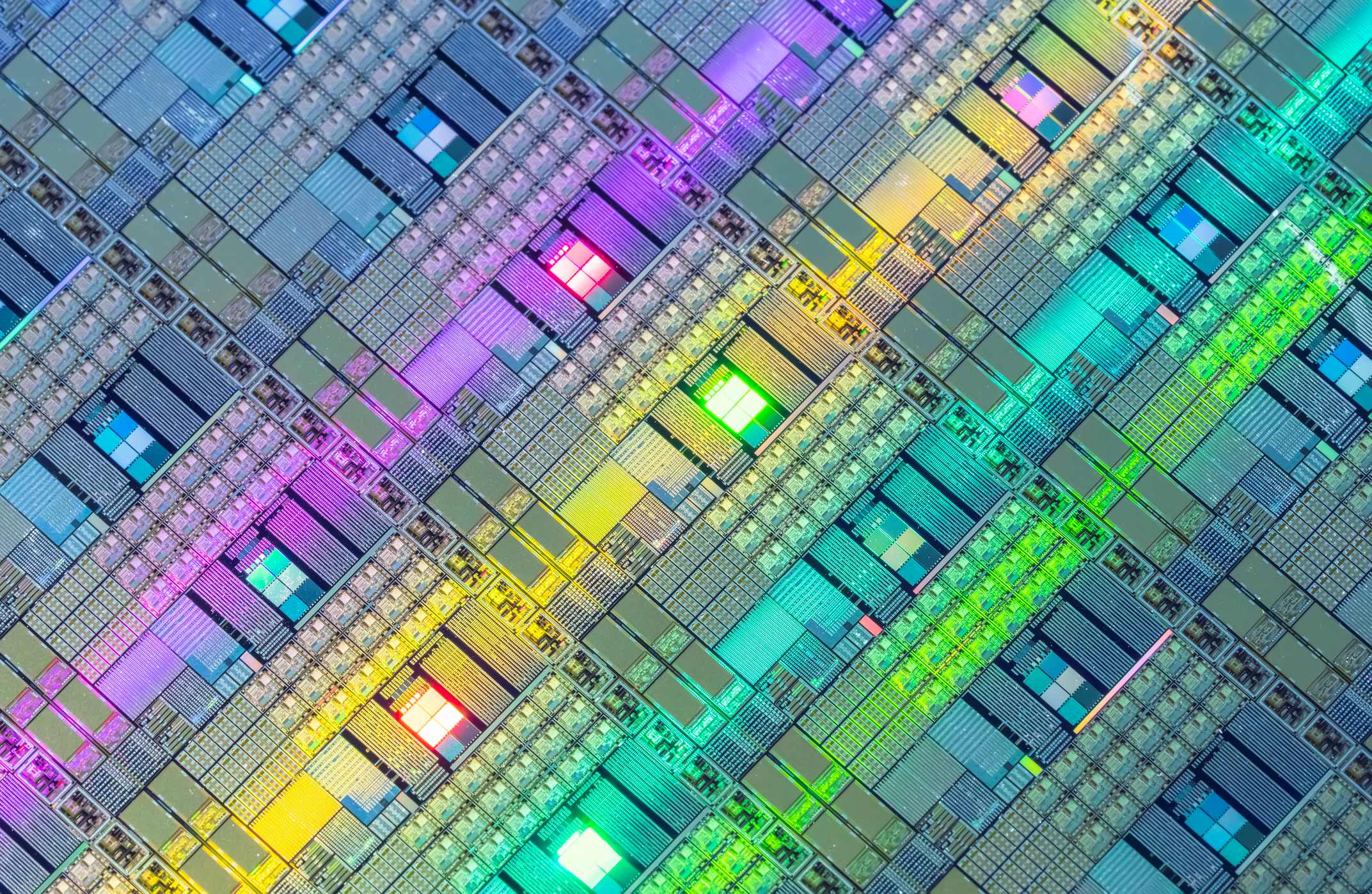
In the last few years, the technology features of ASIC have gotten smaller, while their performance and complexity has increased. The result is that the packaging concept has become increasingly important. Some applications are demanding even more out of their current chip solutions, and packaging is the interface to get access to the chip features and should not degrade chip performance.
Historically, ASIC packaging represented just one step in a long and linear manufacturing process. It was viewed as a stage that came after the design phase. Now, it happens in conjunction with the design phase. An important reason is to ensure that projects are delivered timely: if the packaging phase cannot immediately follow the tape-out, silicon can be idle for months.
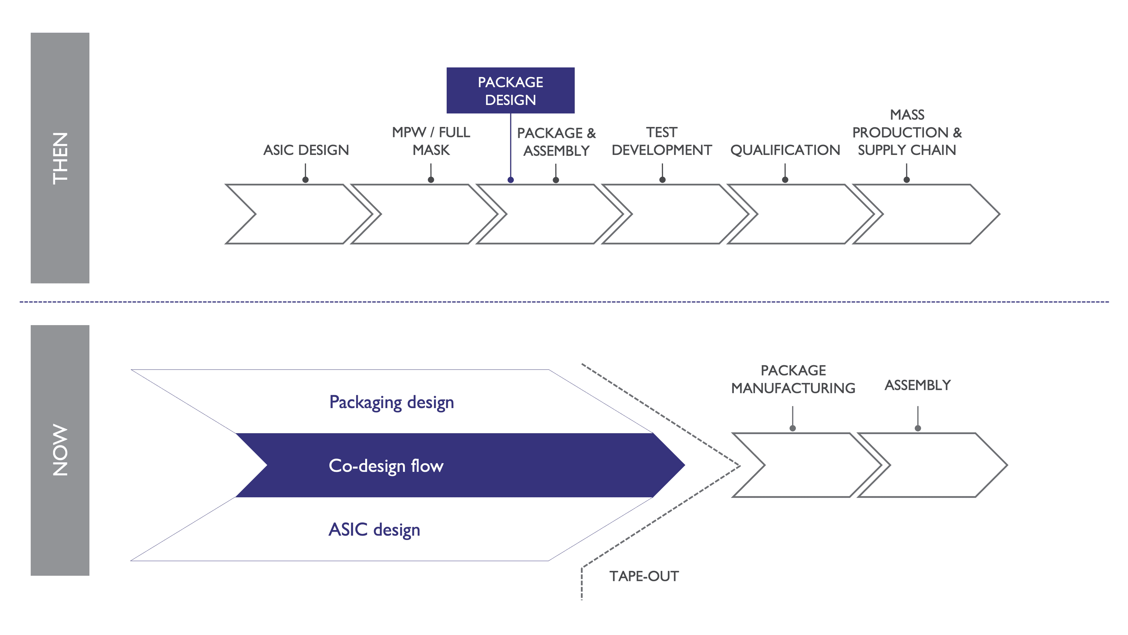
Today, packaging design and ASIC design happen at the same time, whereas previously packaging design was a step that came after production.
A co-design flow of packaging and ASIC design allows customers to evaluate and balance the many factors at play. A co-design flow also helps ensure that the final product delivers the required performance to achieve the intended outcomes. From a performance perspective, the packaging itself should be considered equally important to the ASIC chips.
When dealing with advanced constructs, packaging is not something you consider after the fact, or at the end of your silicon flow. It must be solidified up front, as part of the initial specification and IP selection processes. Selection of IP has an impact, and can both drive you into a certain packaging solution or restrict you from using others.
Watch our recent packaging webinar
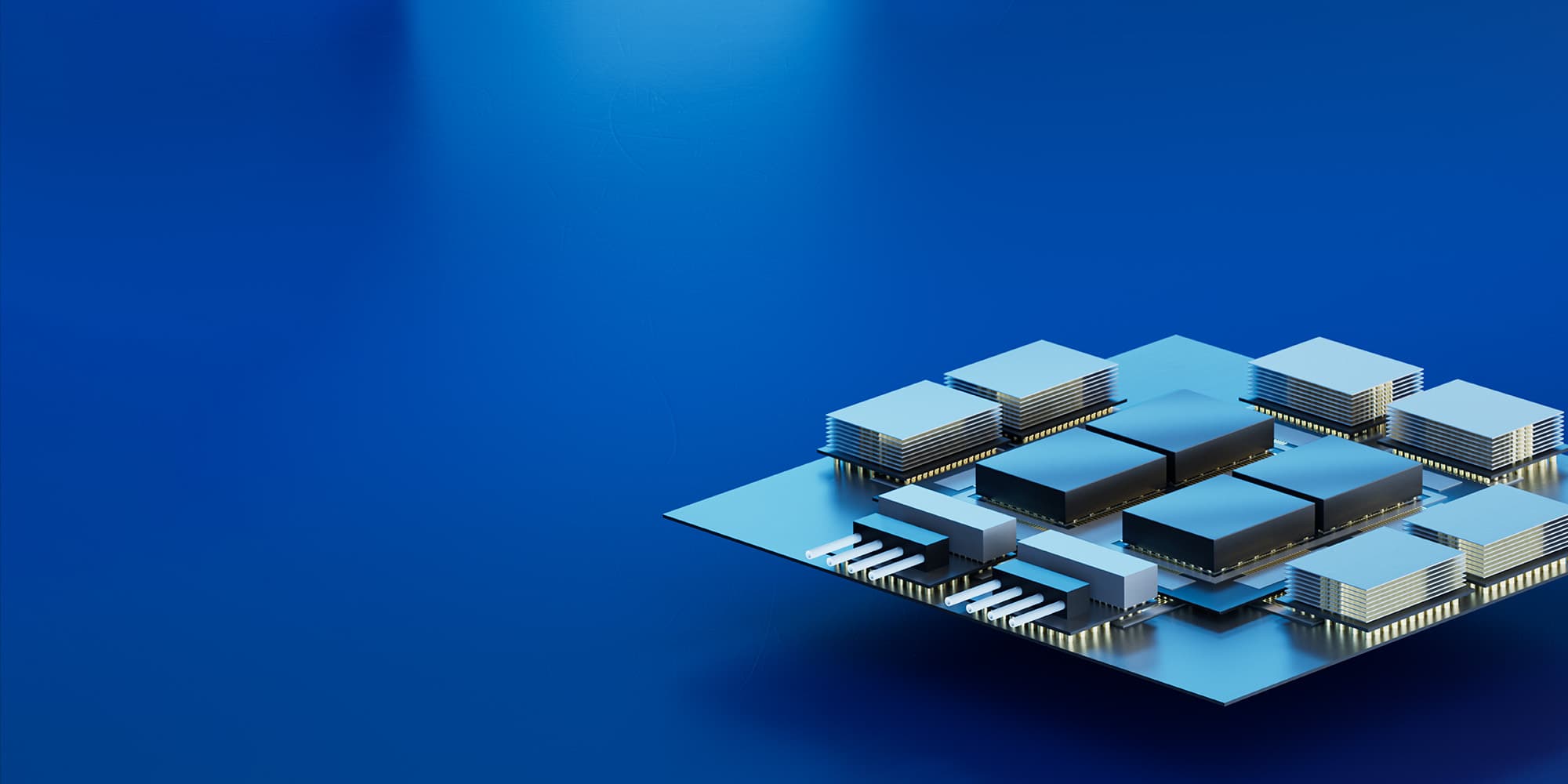
The spectrum of packaging techniques is broad. Where your project maps to that spectrum depends on its complexity and the outcomes you intend to drive. Mainstream packaging techniques are simple and well elaborated, and span from simple QFNs over Ball Grid Array (BGA), Land Grid Array (LGA), Wafer-Level Chip Scale (WLCSP), System in Package (SiP), to Multichip Module (MCM).
Advanced packaging is way more complex, and addresses 2.5D and 3D integration. The primary difference between 2.5D and 3D integration is how the prime dies are positioned in relation to each other. In 2.5D designs, the dies sit side by side and are connected by a silicon or organic interposer. For 3D designs, the dies are stacked and connected by through-silicon vias.

3D packaging has dies stacked on top of each other and connected by through-silicon vias, whereas 2D packaging has the dies next to each other and are connected by interposers.
There is no simple way to decide when or what to use. A high-level feasibility study is to be conducted at the very early stage in the project to explore the PPA (power/performance/area) trade-offs and narrow down the applicable packaging solutions.
Choosing the right ASIC package design for your project
Once your feasibility study is complete, selecting the best packaging option becomes a delicate balancing act of four key factors: cost, reliability, performance and technology restrictions, including silicon and package design.

Cost: There are simple BGAs that cost as little as a few US dollars a piece, sometimes even less depending on the complexity, number of layers and substrate materials involved. Conversely, complex 2.5 or 3D integration can cost hundreds or even thousands of dollars each from a packaging perspective alone.
Performance: Simple BGAs can easily handle performance requirements in the 100s of Mbps range. But if your project requires a data rate in the high 10s of Gbps, the only way to achieve that is with 2.5 or 3D integration. Another performance aspect is the power dissipation where the package that is chosen should be able to handle the dissipated power and thermo-mechanical solutions may need to be applied.
Reliability: Simple BGAs have proven their capabilities and reliability through long-term deployment at scale. They therefore typically represent the lower risk solution. Most advanced packages are much newer to market, and carry a higher reliability risk. That is why an extensive reliability test may need to be executed before going to volume production.
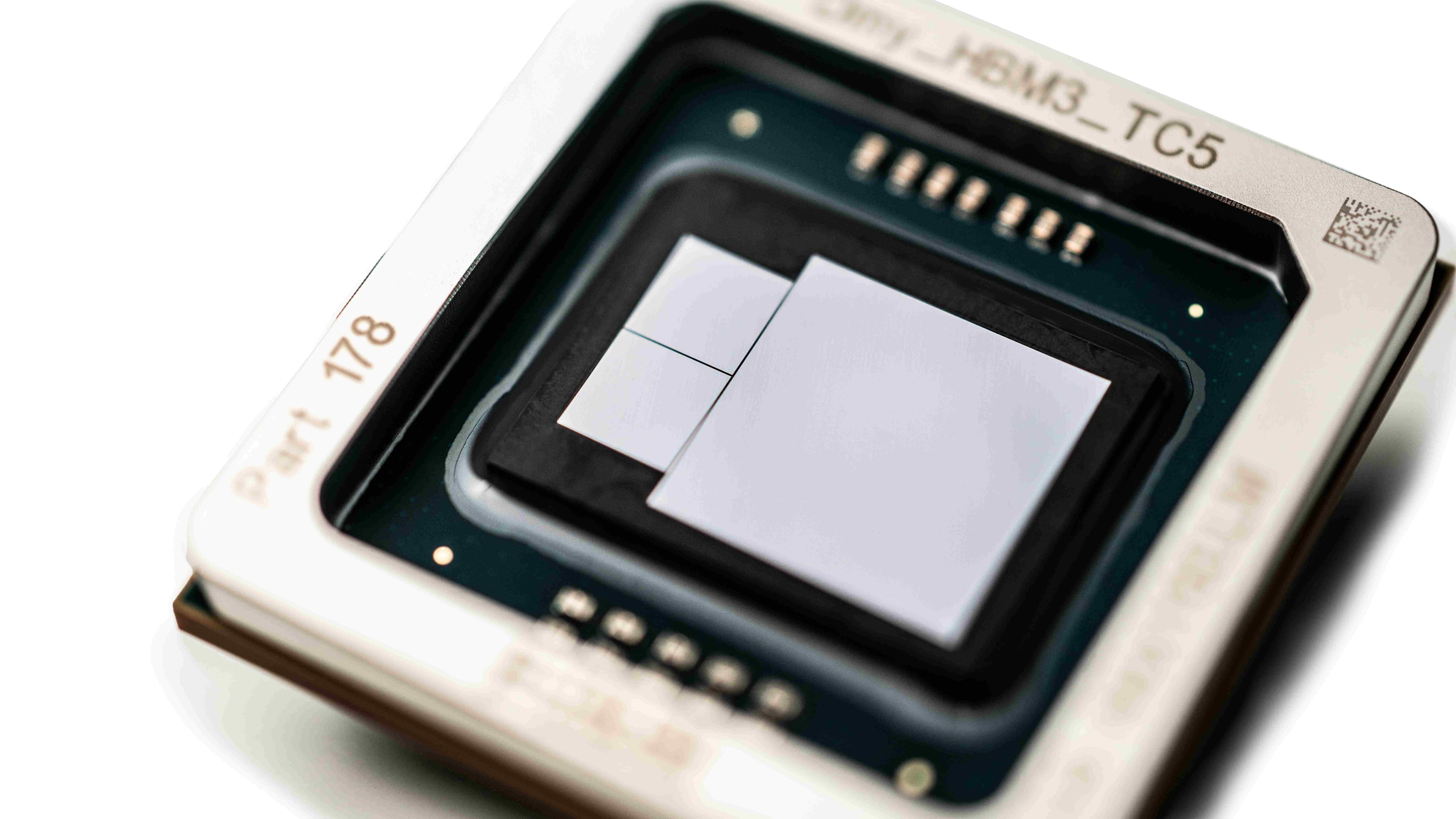
Silicon design: The type of interfacing being used and deployed can push your project toward one or the other end of the spectrum. Standard UCIe interfacing solutions will still fit to the more traditional BGA. Deployment of UCIe advanced interfacing and/or use of HBMs (High Bandwidth Memory), will drive you towards the use of advanced packaging solutions. This creates a need for silicon or RDL (re-distribution layer) interposers, which will typically require a 2.5/3D packaging construct.
Package design: Simple BGAs are sufficient for any project requiring a bump pitch of 125um or higher. Any pitch lower requires silicon or RDL interposers and advanced 2.5/3D packaging solutions.

The general technical range for BGA and 2.5D/3D packaging techniques.
Timing is everything
Another critical consideration is the various manufacturing restrictions that will influence the timeline and success of your project. The silicon fabrication itself typically takes 2-5 months of processing time depending on the technology node selected. This means package materials, interposers and substrate manufacturing must be completed and ready at the moment your silicon leaves the fab to allow for package assembly right after.
For more complex projects, this means having interposers ready, a process that also involves silicon fabrication and carries similar production timelines. Substrates have to be built, a process that varies depending on the complexity of the construction itself and the demand for advanced tools required to manufacture each layer. Average lead time is typically 12-16 weeks, and as long as 30 weeks in times of high demand.
This implies that package design must be finished and approved long before the silicon is complete to ensure alignment between fab production and package construction. It also means that the end package itself becomes another layer of specification that will impact how the actual chip needs to integrate and perform. Once the substrate manufacturing process is underway, the footprint and pin allocation of the silicon design cannot change and instead must adapt to the package design — yet another reason these two processes must happen hand-in-hand to ensure a working finished product.
Those complexities also apply to BGA implementations. But they are more compound when undertaking a 2.5D/3D integration, which requires the alignment of disparate development flows that must ultimately dovetail seamlessly. There are design and production rules for the silicon die itself that must be adhered to, different design rules for the technology used to build silicon interposers, and still different design and manufacturing rules for the substrate. To ensure success requires the capabilities and knowledge to bring all of these different worlds together.
Bringing advanced package design into the real world
From a 3D packaging perspective, there are various technologies that can be used to build the overall design and product. For example, within the TSMC ecosystem, there are two prime distinctions — Chip on Wafer on Substrate (CoWoS), or Integrated Fan-Out (InFO).
Within CoWos, there are three main categories. The prime difference between each is how the space transformer is being constructed and what materials are being deployed at that level. The first two categories are the Si interposer based one (CoWoS-S), which uses a silicon interposer to connect the dies, and the RDL interposer based one (CoWoS-R), which uses an organic interposer to connect the dies. Choosing one over the other depends on performance, die size and interfacing size requirements.
The third category is the Mold-based Interposer (CoWoS-L), which uses a mold interposer to connect the logic die and HBMs. Within that interposer, passive and active elements can be integrated as well. Typically, this means you’re not only combining and integrating the logic die, but also passives such as capacitors and resistors connecting to the substrate to meet the performance of the overall package as required by the design constraints.
Within InFO, connections are typically created by putting packages on top of each other. This includes Package on Package (InFO-PoP) and InFO-OS, which allows for devices to be stacked and logic dies to be embedded in mold.
Take complexity out of the equation with IC-Link
At IC-Link, we have the expertise and resources to help you select the optimal solution for your application, from an ASIC packaging perspective and beyond. We offer a well-resourced, experienced team of design experts able to take into account your different criteria as to select from our offering of a wide range of packaging solutions — from plastic and ceramic, to advanced and even photonics packaging.
Our expertise in assembly and packaging is an integral part of our mission of supporting the silicon manufacturing and supply chain needs of our customers. Any area of expertise you don’t have in-house, we can offer. And because each customer is assigned a specific project manager, you get one point of contact who shields you from all the complexities related to the ASIC packaging process.
For a deeper look at our capabilities, watch our most recent webinar here. Or, if you’d like to learn more about how we can make your next project a success, get in touch.