

Chip development costs, risks, and lead times rise significantly at sub-7nm technology nodes. AI ASIC developers typically assemble systems around their accelerator core from third-party I/O, memory, and interface blocks. The high third-party IP and validation costs associated with subsystems can erode a company’s time-to-market and price advantages. To address the advanced-node design challenge, IC-Link by imec has developed the imec.impulse reference subsystem. This complete design-to-manufacturing solution derisks and accelerates custom AI silicon development at advanced nodes.
Why advanced nodes are raising the stakes for AI chip development
Today’s AI accelerator developers are seeking new approaches to deliver higher performance, lower latency, higher throughput, and better efficiency. At advanced nodes, companies can spend months assembling third-party I/O, memory, and interface third-party IPs.
The hidden costs and risks of integration, verification, and physical design of the subsystem are increasing the barriers to AI chip innovation. These challenges lie well outside the core expertise of most AI chip startups.
Even those with the most advanced core compute IP risk falling behind—not because of their proprietary technology, but rather because of the demands of subsystem design, development, and manufacturing.
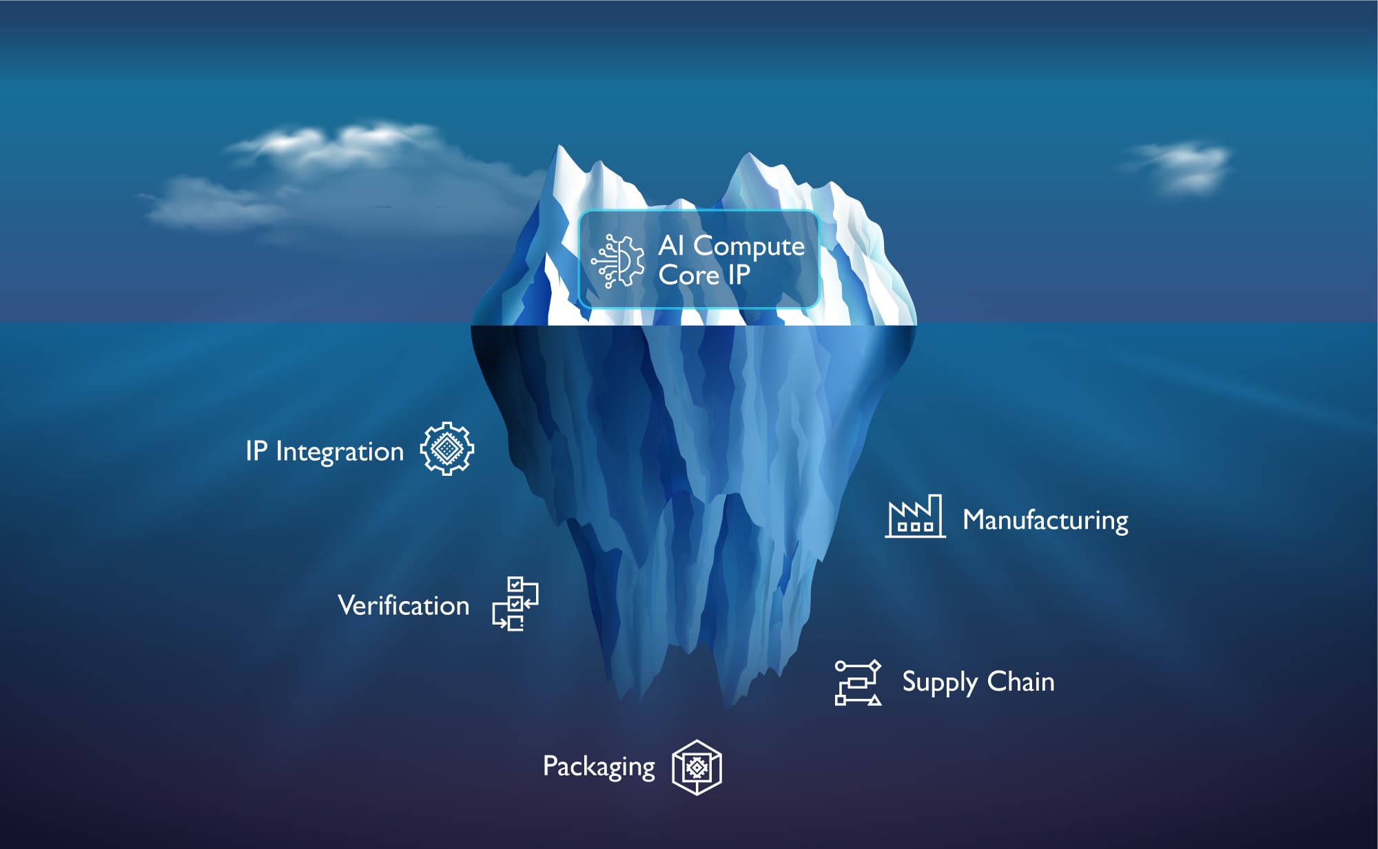
At advanced nodes, the subsystem becomes a major hurdle to AI ASIC development.
Soaring design and mask costs at leading-edge nodes are reshaping AI chip manufacturing economics
Advanced process nodes are upending the traditional cost structure of chip manufacturing, penalizing all but the best-resourced companies. Compared to costs at 28 nm, the cost increases at leading-edge nodes are significant:
- Hardware design costs increase threefold at 7 nm, and fivefold at 3 nm.
- Mask set and wafer costs are multiplied by seven at 7 nm, and fifteen at 3 nm.
- There is an inflection point, where cost per die begins to rise at nodes below 7 nm.
The high cost of third-party I/O IP integration at advanced nodes
Integration with third-party I/O IPs at advanced nodes, another contributor to surging costs and longer lead times, is also a bottleneck for many companies:
- The IP supplier ecosystem is fragmented.
- The non-recurring engineering (NRE) burden is substantial.
- Bring-up across packaging, interfaces, and flows is complex.
In short, tasks like sourcing from third-party IP providers, testing and connecting IP blocks drain engineering resources from a company's differentiator: their proprietary core IP.
Introducing imec.impulse: a complete AI system design-to-manufacturing solution, for reduced risk, cost, and time-to-market
In a departure from conventional approaches, the imec.impulse reference subsystem design allows companies of all sizes to test their core IP with validated I/O IPs selected by IC-Link, removing the burden of:
- Sourcing and testing third-party IPs.
- Rebuilding a new I/O section for each new technology node.
- Integrating IPs from multiple suppliers.
The imec.impulse reference I/O design addresses the challenges of AI ASIC development at advanced nodes by:
- Reducing tape-out and yield risks: IC-Link by imec uses proven IP with a track record of successful tape-outs and takes on all tape-out- and yield-related risks.
- Eliminating the need to navigate the complex ecosystem of third-party IP providers and removing the constraints of IP supply chain management.
- Leveraging IC-Link partnerships with IP providers to reduce third-party IP licensing costs.
- Enabling access to IC-Link’s packaging expertise and manufacturing at TSMC, even for startups and larger companies with small manufacturing volumes.
- Allowing companies to focus on their core IP and increasing speed to silicon, protecting their time-to-market advantage.
With imec.impulse, IC-Link by imec starts with the customer's system specifications, providing front-end (RTL integration and verification) and back-end design (placement & routing, timing closure, physical verification) services, tape-out, advanced packaging and testing, prototyping, and volume production.
IC-Link by imec handles handover from engineering to production and takes full responsibility for the supply chain, freeing companies to focus on their core IP and helping them compete in today’s global market with innovative products manufactured at advanced nodes.
A pre-validated interconnect layer for AI ASICs backed by services from design to manufacturing
Imec.impulse is not a one-size-fits-all fixed-spec IP block. It is a reference subsystem that leverages shared design and engineering efforts in much the same way the automotive industry has utilized standard car architectures and chassis to maximize returns on engineering investments. This proven approach simplifies design, sourcing, and assembly, enabling automotive manufacturers to offer vehicles with a wide range of features that respond to consumer demand while increasing production efficiencies and reducing costs. Today IC-Link has adopted this principle for AI ASIC subsystems.
The imec.impulse reference design reduces subsystem integration complexity at advanced nodes, opening a proven path to innovation that even start-ups can leverage to maintain their competitive advantage. With imec.impulse, IC-Link by imec is an end-to-end solution partner for AI chips at advanced nodes.
Here’s how it works:
- Based on the customer’s system specifications, the imec.impulse subsystem is customized with a selection of silicon-proven third-party IP from IC-Link partners and delivered as an RTL with the target PPA.
- The core AI accelerator processing IP is integrated using IC-Link’s design team.
- AI chip developers can focus their design resources on their core processors.
- The complete system is manufactured through IC-Link by imec’s partnership with TSMC.
Fully adaptable to your product development program, imec.impulse is delivered as a completely transparent RTL design and can be converted to a reusable fixed I/O chiplet for specific nodes.
- This I/O subsystem reference design integrates industry-leading IP (e.g. Arteris) selected and silicon-proven by imec. IC-Link by imec sources third-party IP and negotiates and contracts directly with its IP partners so you don’t have to.
- Complex peripheral subsystems are integrated and tested by IC-Link by imec.
- As IC Link is a member of the TSMC Value Chain Alliance (VCA) and TSMC 3DFabric® Alliance, imec.impulse provides companies with a direct path to manufacturing at advanced nodes and advanced packaging with a global leader. IC-Link manages the tape-out and supply chain—two major complex tasks for a semiconductor company.
Europe's only design partner offering N2P backside power delivery architecture
IC-Link by imec is the only design service provider in Europe developing an N2P backside power delivery subsystem architecture. For imec.impulse customers, this means early engagement with the ecosystem for a direct path toward manufacturing at the most advanced nodes.
Learn how you can leverage the IP, design, and manufacturing advantages of imec.impulse by partnering with IC-Link by imec today.