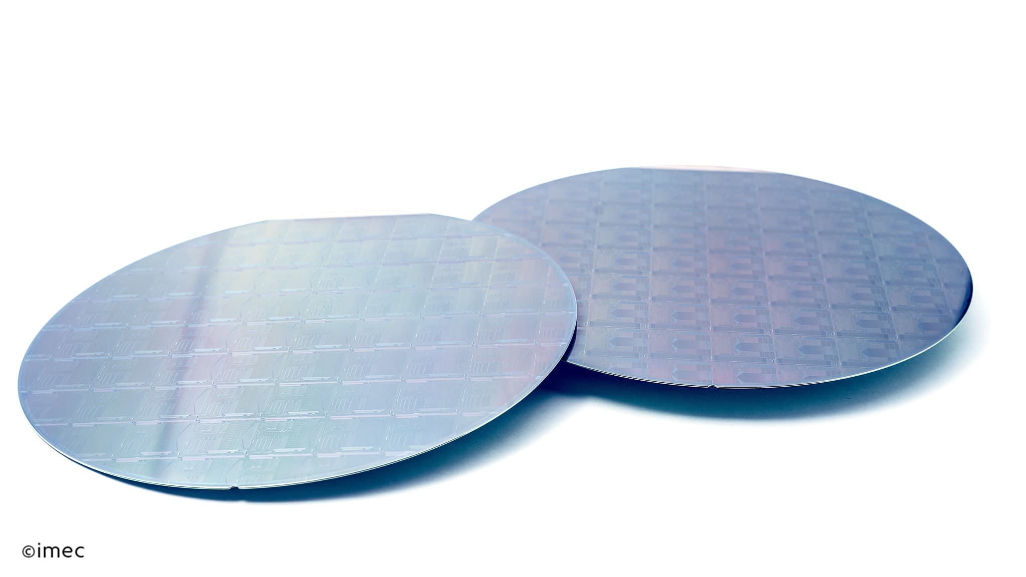
Prototyping and small volume production of SiN photonic ICs
Get affordable access to integrated photonics based on silicon nitride (SiN) through multi-project wafer runs.
Are you working on an application that requires waveguides with extremely low propagation loss? Then silicon nitride might be the perfect material – if only because of its transparency for visible and near-infrared wavelengths.
Moreover, silicon nitride can be easily integrated into a silicon CMOS platform, which opens the door for the creation of photonic integrated circuits (PICs) that address various challenges in domains such as quantum computing, health, beamforming, and so on.
Affordable access to photonic ICs
Developing a PIC requires advanced capabilities. But is accessible to you for prototyping and low-volume manufacturing thanks to imec’s multi-project wafer (MPW) service where you share the expenses for photomasking and processing with other designers.
Click here for a schedule of the upcoming runs and pricing details.
For the design of your PIC, we offer a process design kit (PDK) that’s compatible with photonics design software of Synopsis and Luceda Photonics. You also have access to a growing collection of designs for photonic components that were developed and validated by the EU project PIX4life.
Our MPW services are provided through the EUROPRACTICE platform, where imec is one of the partners.
Apart from the MPWs, we also offer low- or mid-volume dedicated runs that give you more opportunity for customization.